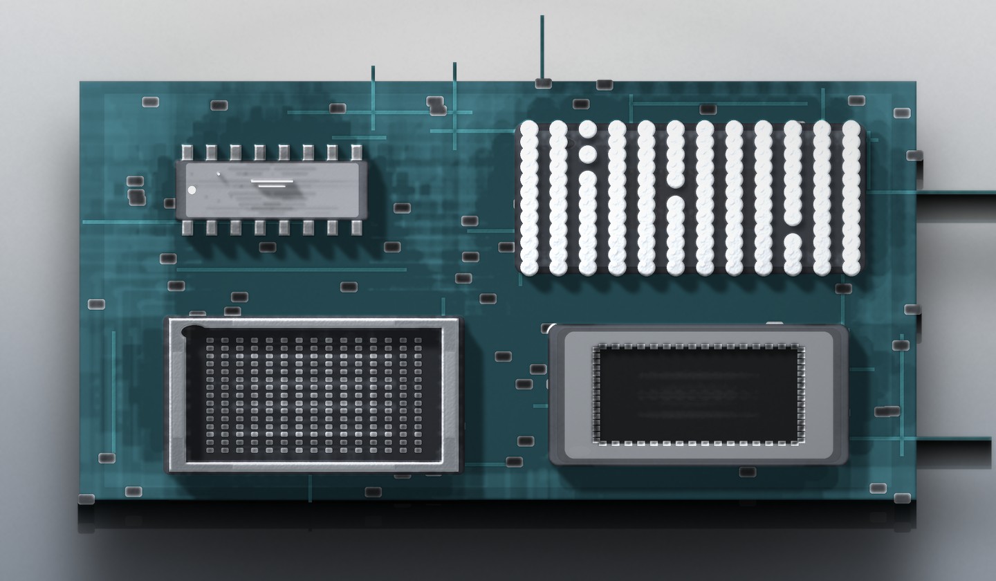
Choosing between 2.5D and 3D packaging comes down to evaluating interconnect density, thermal constraints, available package area, and manufacturing readiness. 2.5D architectures place dies side by side and connect them through high-density lateral routing - an approach that scales well for chiplet-based processors and high-bandwidth memory (HBM). 3D packaging stacks active dies vertically, enabling tighter coupling and a smaller footprint but introducing more demanding thermal and assembly challenges. Neither approach is inherently superior; the right choice depends on bandwidth requirements, power density, cooling capability, yield expectations, and total system cost. Many advanced systems now combine both methods, using vertical integration where extremely short connections matter and lateral integration where thermal access and scalability are priorities.

Structural and Interconnect Differences
The fundamental distinction lies in how active dies are positioned and connected. In 2.5D packaging, multiple dies occupy the same horizontal plane and communicate through an intermediate routing structure - typically a silicon interposer, redistribution layer (RDL), or localized silicon bridge. This lateral arrangement keeps dies physically separate while enabling dense, short-path connections across the package.
3D packaging introduces a vertical dimension by placing one or more active dies directly above or below others. Connections between stacked layers use fine-pitch microbumps, hybrid bonding, or through-silicon vias (TSVs) where signals must traverse a die. The result is a compact assembly with very short vertical interconnects, though thermal and manufacturing complexity increase.
Importantly, not every 2.5D package relies on a full silicon interposer, and not every 3D stack requires TSVs throughout. Modern implementations mix techniques based on signal density, power delivery, and cost constraints.
| Factor | 2.5D Packaging | 3D Packaging |
|---|---|---|
| Die arrangement | Side by side on a common plane | Vertically stacked |
| Interconnect structures | Silicon interposer, RDL, embedded bridge, microbumps | Microbumps, hybrid bonding, TSVs where needed |
| Connection path length | Short lateral paths between adjacent dies | Very short vertical paths between layers |
| Interconnect density | High, limited by interposer or RDL pitch | Potentially higher with fine-pitch vertical bonding |
| Package footprint | Larger horizontal area | Reduced horizontal footprint |
| Thermal access | More direct cooling paths to each die | Heat removal complicated by stacking |
| Manufacturing complexity | Depends on interposer size, routing density, and die count | Often higher due to thinning, alignment, and bonding |
| Common applications | Chiplet processors, HBM-equipped GPUs, AI accelerators | Stacked logic, tightly coupled functions, area-constrained systems |
How 2.5D Packaging Works
2.5D packaging integrates multiple semiconductor dies into a single package by connecting them through a high-density intermediate layer. The dies themselves remain in a single horizontal plane rather than being stacked directly on top of one another.
A typical signal path in a silicon-interposer-based 2.5D package follows this sequence:
Die A → Microbump → Silicon interposer routing → Microbump → Die B
The interposer contains fine-pitch metal interconnects that carry signals between neighboring dies at densities far exceeding what conventional package substrates or printed circuit boards can support. Where connections must pass from the interposer to the package substrate below, TSVs can provide vertical electrical paths through the interposer silicon.
However, 2.5D architectures are not limited to full silicon interposers. Alternative implementations include:
- RDL interposers: Use redistribution layers built on an organic or glass substrate to route signals between dies.
- Embedded bridges: Small pieces of silicon with dense routing are placed only where high-bandwidth die-to-die connections are required, reducing cost compared to large interposers.
This flexibility allows 2.5D packaging to scale from chiplet processors with modest interconnect needs to GPU and AI accelerator packages connecting multiple compute dies and several HBM stacks.

How 3D Packaging Works
3D packaging places active semiconductor dies in a vertical stack, enabling direct die-to-die communication through the shortest possible physical path. Instead of routing signals laterally across an interposer, connections pass directly between adjacent layers.
A simplified 3D assembly structure looks like this:
Upper active die
↓ Fine-pitch interconnect (microbumps or hybrid bonding)
Lower active die or base die
↓ Package-level connections
Package substrate
Connections between stacked dies can use microbumps - small solder bumps with pitches typically ranging from 40 µm down to below 10 µm - or hybrid bonding, which directly bonds metal and dielectric surfaces without solder, enabling even finer pitch and lower resistance. TSVs may also be present to carry signals, power, or ground through a die when connectivity must extend beyond immediately adjacent layers.
TSVs are an enabling technology for many 3D architectures, but they do not define 3D packaging. A two-die stack connected by microbumps or hybrid bonding, with no TSVs in the upper die, is still a 3D package.
The primary advantage of this approach is integration density. Many parallel connections can fit within a small horizontal area, and communication latency can be minimized by eliminating long lateral routes. The tradeoff is increased thermal coupling between stacked heat sources and more demanding assembly and testing processes.

Performance and Design Tradeoffs
Bandwidth, Latency, and Interconnect Density
Both 2.5D and 3D packaging reduce connection lengths compared to traditional multi-package PCB-based systems. Shorter interconnects generally support higher data rates, lower latency, and improved signal integrity.
2.5D packaging enables wide, high-bandwidth interfaces between processors and memory or between multiple chiplets. HBM integration in GPUs and AI accelerators relies on 2.5D interposer connections to provide aggregate memory bandwidth exceeding 1 TB/s in current implementations.
3D packaging can achieve even higher interconnect density by leveraging vertical stacking. Fine-pitch hybrid bonding can deliver thousands of connections per square millimeter, enabling tightly coupled logic layers or cache dies placed directly above processing cores.
However, raw interconnect count does not automatically translate to higher effective bandwidth. Actual performance depends on interface protocol design, clocking, signal integrity, power delivery, and how well the physical interconnect matches the communication pattern of the application.
Power Efficiency and Signal Integrity
Shorter interconnects reduce parasitic capacitance, resistance, and inductance. For memory interfaces moving large amounts of data, this can significantly lower I/O power consumption. A typical off-package DDR or LPDDR interface might consume several picojoules per bit, while an on-package HBM interface connected via 2.5D interposer can reduce this to well below 1 pJ/bit.
Total system power still depends on many factors beyond packaging, including memory architecture, logic power, data movement patterns, and workload characteristics. Packaging improvements reduce interconnect overhead but do not eliminate power consumption from computation, memory access, or on-die communication.
Higher interconnect density also introduces signal integrity challenges. Crosstalk between closely spaced signal lines, simultaneous switching noise, power delivery network impedance, and electromagnetic coupling all become more pronounced as pitch decreases. Both 2.5D and 3D designs require careful modeling, simulation, and layout optimization to maintain signal quality.
Package Footprint
2.5D packaging arranges dies laterally, so adding more dies or increasing die size directly increases the required interposer or substrate area. Large interposers can become expensive, and very large packages can face yield challenges during fabrication and assembly.
3D packaging stacks dies vertically, reducing the horizontal footprint. This is valuable in space-constrained applications such as mobile devices, compact edge computing systems, or high-density server designs where board area is limited.
The smaller footprint comes at the cost of increased design complexity, more demanding thermal management, and tighter manufacturing tolerances. A 3D package is not automatically more cost-effective simply because it occupies less board space.
Thermal Management
Thermal behavior is one of the most significant practical differences between 2.5D and 3D packaging.
In a 2.5D layout, high-power dies are positioned side by side with independent thermal paths to the package lid or heat spreader. While neighboring dies can influence one another through substrate conduction and shared cooling, each die typically has relatively direct access to the cooling interface. This makes 2.5D packaging well-suited to processors and GPUs that generate tens to hundreds of watts.
3D packaging concentrates multiple heat sources in a vertical stack. Heat generated by an internal die must pass through bonding interfaces, silicon layers, and any intervening structures before reaching the cooling surface. This increases thermal resistance and can create significant temperature gradients between stacked dies. Thermal coupling also means that power consumption in one layer affects junction temperature in adjacent layers.
Effective 3D thermal management strategies include:
- Stacking lower-power dies on top of high-power dies
- Thinning upper dies to reduce thermal resistance
- Using thermal TSVs to improve vertical heat conduction
- Applying advanced cooling solutions such as embedded microfluidic channels or direct liquid cooling
- Carefully managing power states and workload distribution across stacked dies
For systems where multiple high-power compute dies must be integrated, 2.5D packaging often provides a more manageable thermal solution.
Manufacturing, Yield, Testing, and Cost
Manufacturing Complexity
2.5D packaging manufacturing involves several specialized processes:
- Fabricating silicon interposers with fine-pitch through-silicon vias and metal routing layers
- Depositing microbumps on both the dies and the interposer
- Aligning and bonding multiple dies to the interposer with micron-level precision
- Attaching the interposer assembly to an organic package substrate
- Underfill deposition and curing to provide mechanical support and moisture protection
RDL-based 2.5D approaches replace the silicon interposer with polymer dielectric and copper redistribution layers, which can reduce cost but may limit routing density and electrical performance.
3D packaging introduces additional complexity:
- Thinning dies to thicknesses often below 50 µm to reduce thermal resistance and enable vertical stacking
- Aligning stacked dies with sub-micron accuracy for hybrid bonding or fine-pitch microbumps
- Managing stress and warpage during stacking and bonding
- Ensuring reliable TSV formation, metallization, and isolation where TSVs are used
- Controlling thickness uniformity across wafers to enable repeatable bonding
Both approaches require advanced equipment, tight process control, and skilled engineering. Neither is inherently easier to manufacture; complexity depends on specific design requirements, die sizes, interconnect pitch, and the number of components in the package.
Yield and Known-Good Die
In any multi-die package, overall yield depends on the yield of each individual die, the interconnect formation yield, the assembly process yield, and final package test yield. A single defective die can render an entire expensive package non-functional.
Known-good die (KGD) strategies test individual dies at the wafer level before assembly. Dies that pass electrical testing are marked as known-good and selected for integration. This reduces the probability of assembling defective dies into high-value packages but adds wafer-level test cost and requires testability features such as probe pads or built-in self-test circuits.
As the number of dies in a package increases and individual die costs rise - especially for advanced logic dies fabricated on leading-edge nodes - KGD screening becomes economically essential. However, wafer-level testing cannot always replicate final package operating conditions, so some defects may only become apparent after assembly.
Yield also depends on interconnect reliability. Microbump formation, underfill voids, hybrid bonding defects, TSV failures, and interposer routing opens or shorts can all reduce package yield. For this reason, 2.5D packaging does not automatically have higher yield than 3D packaging; actual yield depends on process maturity, design margins, and manufacturing control for the specific implementation.
Testing Challenges
Advanced packages require testing at multiple stages:
- Wafer-level test: Electrical screening of dies before dicing
- KGD test: More comprehensive die-level testing after dicing but before assembly
- Post-bond test: Testing after die attachment to interposer or after stacking
- Final package test: Electrical validation of the completed package
- System-level test: Validation in the target system environment
Testing becomes more difficult as integration density increases. In 3D stacks, internal dies and interfaces may become inaccessible after bonding. This makes pre-bond testing, design-for-test features, and built-in self-test (BIST) circuits increasingly important.
Test access also affects debug and failure analysis. If a packaged device fails, isolating the defect to a specific die, interconnect, or interface can be challenging, especially in 3D structures where physical access to internal layers is limited.
Cost Considerations
Neither 2.5D nor 3D packaging is inherently lower cost. Total cost depends on:
- Die cost: Leading-edge logic dies fabricated on 3 nm or 2 nm nodes are expensive; mature-node I/O or memory chiplets are less expensive
- Interposer or substrate cost: Large silicon interposers add significant cost; RDL and bridge-based approaches can reduce this
- Assembly cost: Fine-pitch bonding, alignment, underfill, and stacking all require specialized equipment and longer process times
- Test cost: Wafer-level screening, KGD testing, and final package testing add cost per device
- Yield loss: Defective dies, interconnect failures, and assembly defects reduce effective yield and increase cost per good unit
- Thermal management cost: Advanced cooling solutions such as vapor chambers, liquid cooling, or custom heat spreaders add cost
- Volume: High-volume production can amortize tooling and development costs; low-volume production carries higher per-unit overhead
A more expensive packaging approach may still be economically justified if it enables higher system performance, greater energy efficiency, or capabilities that cannot be achieved with discrete components on a PCB. The relevant comparison is total system cost and value, not packaging cost in isolation.
Applications and Industry Adoption
HBM and AI/HPC Systems
High-bandwidth memory (HBM) demonstrates how 2.5D and 3D packaging can coexist in a single system.
An HBM stack consists of multiple DRAM dies stacked vertically and connected through TSVs - a 3D memory architecture. Each HBM stack includes a base die with a wide I/O interface, typically 1024 bits per stack.
At the package level, multiple HBM stacks are placed around a GPU or AI accelerator die and connected via a silicon interposer or similar 2.5D structure. This lateral integration provides the wide parallel interfaces needed for aggregate memory bandwidth exceeding 1 TB/s while keeping the high-power processor die thermally accessible.
A single advanced GPU package can therefore contain:
- A large compute die (or multiple compute chiplets) fabricated on a leading-edge node
- Multiple HBM stacks, each internally a 3D structure
- 2.5D interposer connections between compute and memory
- Package substrate, power delivery network, and thermal solution
This hybrid architecture delivers the bandwidth benefits of 3D memory integration without requiring the processor die to be stacked vertically, which would create unmanageable thermal conditions.
Chiplet-Based Processors
Chiplet architectures disaggregate a large monolithic processor into smaller functional blocks - compute cores, I/O, memory controllers, cache - that can be fabricated on different process nodes and connected within a package.
2.5D packaging enables chiplet integration by providing high-bandwidth, low-latency die-to-die interconnects. AMD's EPYC processors use chiplets connected through an organic substrate with short die-to-die routing. Intel's compute products use Embedded Multi-die Interconnect Bridge (EMIB), which places small silicon bridges with dense routing only where high-bandwidth connections are required, avoiding the cost of a full interposer.
Chiplet-based designs offer several advantages:
- Smaller dies have higher yield on advanced nodes
- Mature-node I/O and memory controllers can be combined with leading-edge compute
- Defective chiplets can be discarded without scrapping an entire large die
- Different chiplet configurations can be assembled to create product variants
However, chiplet integration also introduces challenges in power delivery, clock distribution, thermal management, and ensuring reliable die-to-die communication across manufacturing variation.
Other Applications
Advanced packaging is also appearing in:
- Networking ASICs: Integrating SerDes, packet processors, and switching logic with high-speed interfaces
- Mobile processors: 3D packaging can reduce footprint in smartphones and tablets, though thermal constraints limit how much high-power logic can be stacked
- Automotive systems: Safety-critical and AI-accelerated automotive computing can benefit from chiplet-based modularity and integration density
- Edge AI accelerators: Compact 3D packages can deliver high performance in thermally constrained edge devices with active cooling
Each application has distinct requirements for bandwidth, power, thermal limits, reliability, and cost, which determine whether 2.5D, 3D, or hybrid packaging is most appropriate.
Selection Criteria and Decision Framework
Define Bandwidth and Latency Requirements
Start by identifying which components exchange the most data and which communication paths are performance-critical. A processor with multiple HBM stacks requires very wide interfaces, favoring lateral 2.5D integration. Two tightly coupled logic blocks that must share cache or communicate at very high frequency may benefit more from vertical 3D stacking.
Quantify the required bandwidth, latency, and interface width for each die-to-die connection. This determines whether standard substrate routing, 2.5D interposer or bridge connections, or 3D vertical interconnects are necessary.
Map Chiplets and Interfaces
Create a physical and logical map of all dies in the package and their communication requirements. Identify:
- Which dies communicate with which others
- The bandwidth and latency requirements for each interface
- Power delivery and ground return paths
- Thermal characteristics and power dissipation of each die
This prevents designing the package around a single high-bandwidth interface while neglecting other connections that may determine overall system performance.
Evaluate Package Area Constraints
Determine the maximum allowable package size based on the target system's board area, socket or connector dimensions, and mechanical constraints. If all required dies fit comfortably in a lateral layout, 2.5D integration avoids the complexity of stacking. If package area is tightly constrained, 3D integration may be necessary despite added thermal and manufacturing challenges.
Assess Thermal Limits and Cooling Capability
Estimate the power dissipation of each die and the total package power. Perform thermal simulations to understand junction temperatures, thermal gradients, and hotspot locations under representative workloads.
For packages with multiple high-power dies, 2.5D layouts typically provide better thermal management. If thermal constraints are manageable - for example, if only one die generates significant power, or if advanced cooling is available - 3D integration may be feasible.
Thermal analysis should happen early in the architecture phase. Discovering late in the design cycle that a 3D package cannot be adequately cooled can require expensive redesigns or compromise performance.
Check Manufacturing and Supply Chain Readiness
Determine which packaging technologies are accessible through available manufacturing partners. Relevant capabilities include:
- Maximum interposer size and TSV density
- RDL routing layers and pitch
- Availability of silicon bridge technology
- Microbump pitch and process maturity
- Hybrid bonding capability and alignment tolerance
- Die thinning capability and thickness uniformity
- Assembly equipment and process control for multi-die packages
A package design that exceeds available manufacturing capability will face schedule delays, yield problems, or may not be manufacturable at all.
Plan for Testing and Yield
Define a test strategy that includes:
- Wafer-level screening to identify defective dies
- KGD testing for high-value dies before assembly
- Post-bond electrical test where feasible
- Final package test to validate all interfaces and functionality
- Failure analysis access and debug capability
As package value increases, KGD screening becomes essential. For very high-value packages, testing cost per device can be substantial, but the cost of assembling a defective die into a package is higher.
Compare Total System Cost and Value
Evaluate packaging cost in the context of total system cost and the value delivered. Consider:
- Die cost for each component
- Packaging materials, assembly, and test cost
- Expected yield and yield loss cost
- Thermal solution cost
- The performance, bandwidth, power efficiency, or density advantage provided by advanced packaging
- Whether the packaging approach enables capabilities that cannot be achieved with standard packaging
In many cases, a higher packaging cost is justified by system-level benefits. The relevant question is not which packaging approach is cheaper, but which delivers the best overall value for the target application.
Combining 2.5D and 3D Integration
Modern advanced packages increasingly combine lateral and vertical integration within a single system. Different parts of a package can use the integration method best suited to their specific requirements rather than forcing every connection into a single architecture.

Why Hybrid Architectures Are Useful
A high-performance computing package might include:
- A 3D stack of cache dies placed directly above compute cores to provide very high bandwidth and low latency
- Multiple HBM stacks, each internally a 3D structure, positioned laterally around the processor
- 2.5D interposer or bridge connections between the processor and HBM stacks
- Separate I/O chiplets connected via the same lateral interconnect
This approach provides dense vertical integration for tightly coupled logic and cache while using lateral integration for memory and I/O, where thermal access and wide interfaces are more important than vertical compactness.
Hybrid architectures allow engineers to optimize each part of the package independently. The design question becomes where to apply 2.5D integration and where to apply 3D stacking, rather than choosing a single approach for the entire package.
Design and Manufacturing Considerations
Combining 2.5D and 3D integration increases design complexity. Engineers must manage:
- Multiple die-to-die interfaces with different electrical and mechanical characteristics
- Power delivery and ground return paths through both lateral and vertical structures
- Thermal coupling between stacked dies and lateral thermal spreading to neighboring components
- Assembly process flows that may involve both interposer bonding and vertical stacking
- Test access and debug strategies for components that may be partially or fully obscured after assembly
However, the additional design complexity can be justified by the system-level performance and efficiency benefits. As tools, processes, and design methodologies mature, hybrid 2.5D/3D architectures are becoming more common in high-performance computing, AI acceleration, and advanced networking products.
Conclusion
2.5D and 3D packaging are not competing alternatives where one will eventually replace the other. They are complementary integration strategies that address different design requirements. 2.5D packaging excels at integrating multiple large dies, providing wide high-bandwidth interfaces, and maintaining manageable thermal conditions - making it well-suited to chiplet processors and HBM-equipped GPUs. 3D packaging enables very high interconnect density, short vertical connections, and reduced package footprint, but introduces greater thermal and manufacturing complexity.
The best packaging approach depends on bandwidth requirements, power density, thermal constraints, available package area, manufacturing capability, yield expectations, and total system cost. In many advanced systems, the most effective solution combines both methods, using vertical integration where extremely tight coupling is required and lateral integration where thermal access, scalability, or wide parallel interfaces are priorities. Understanding the fundamental tradeoffs and design constraints allows engineers to select or combine packaging technologies that best meet their system's specific requirements.
Frequently Asked Questions
What is the fundamental difference between 2.5D and 3D packaging?
2.5D packaging connects multiple dies positioned side by side through a high-density lateral routing structure such as a silicon interposer, RDL, or bridge. 3D packaging stacks active dies vertically and connects them through fine-pitch interconnects such as microbumps or hybrid bonding, often with very short vertical signal paths.
Does every 2.5D package use a silicon interposer?
No. 2.5D architectures can also use RDL-based interposers or embedded silicon bridges. The choice depends on required routing density, die sizes, performance targets, and cost constraints. Full silicon interposers provide the highest routing density but are expensive for large packages.
Does every 3D package rely on through-silicon vias?
No. TSVs are used when signals, power, or ground must pass through a die, but many 3D packages connect adjacent stacked dies using only microbumps or hybrid bonding without TSVs in the upper die. TSVs are an enabling technology for some 3D architectures but do not define 3D packaging.
Why is thermal management more challenging in 3D packaging?
Stacking multiple active dies vertically concentrates heat sources in a small volume and increases thermal resistance between internal dies and the cooling surface. Heat generated by a buried die must pass through bonding interfaces and silicon layers before reaching the heat spreader or cooler, creating temperature gradients and thermal coupling between layers.
Is HBM considered 2.5D or 3D packaging?
HBM is a 3D stack of DRAM dies connected by TSVs within each memory device. However, HBM stacks are typically placed laterally around a processor and connected via 2.5D interposer or bridge structures. A single package containing HBM therefore combines 3D memory integration with 2.5D processor-to-memory connections.
Which packaging approach is better: 2.5D or 3D?
Neither is universally better. 2.5D packaging is often preferred when multiple large dies, HBM, and manageable thermal conditions are required. 3D packaging is advantageous when very high interconnect density, extremely short connections, and reduced package footprint justify the added thermal and manufacturing complexity. The best choice depends on the specific requirements of bandwidth, latency, power, thermal limits, package area, manufacturing capability, yield, and cost. Many advanced systems now combine both approaches within a single package.