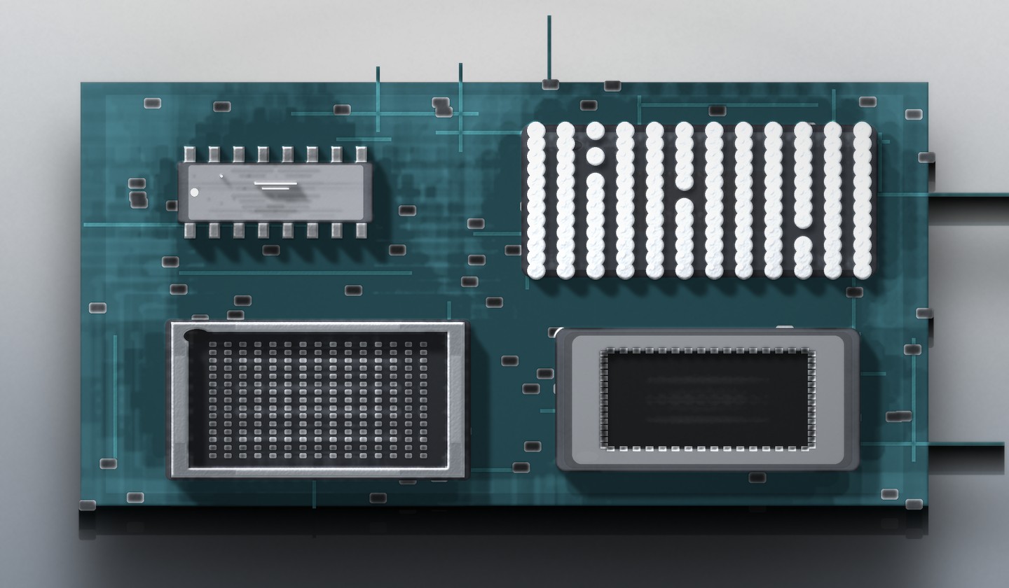
Choose 2.5D packaging when you need wide lateral connections between chiplets and HBM with accessible thermal paths; choose 3D when vertical density and the smallest possible footprint justify stacking complexity. The real question isn't which is better - it's which tradeoffs your system can afford, because thermal limits, manufacturing capability, and yield management often decide before bandwidth does.
Key Takeaways:
- 2.5D places dies side by side and connects them through silicon interposers, RDL structures, or bridges; 3D stacks dies vertically with microbumps or hybrid bonding - but many real systems combine both.
- HBM integration is the clearest case for 2.5D: processors need wide interfaces to multiple memory stacks, and keeping high-power dies lateral makes cooling far more practical.
- 3D stacking concentrates heat in a smaller volume, and internal dies sit farther from the cooling surface - this matters more than most early-stage architecture discussions acknowledge.
- Yield management becomes critical in both approaches as chiplet count rises; screening dies before integration reduces the risk of assembling expensive failures, but post-bond test access in 3D stacks remains a hard problem.
- Neither approach costs less by default - large silicon interposers are expensive, but 3D bonding, thinning, alignment, and thermal solutions add cost quickly.
What Defines 2.5D and 3D Packaging
2.5D packaging connects multiple dies placed side by side using a high-density interconnect layer beneath them. The most recognized implementation uses a silicon interposer: a passive silicon structure with fine metal routing that carries signals between neighboring dies at much higher density than a conventional organic substrate allows. Through-silicon vias (TSVs) in the interposer connect its routing layers to the package substrate below.
But not every 2.5D package uses a full silicon interposer. RDL (redistribution layer) interposers replace silicon with polymer and copper routing, trading some interconnect density for lower cost and larger area capability. Localized silicon bridges - small strips of dense routing embedded in an organic substrate - provide high-density connections only where needed, avoiding the expense of a full interposer.
A typical signal path in 2.5D packaging:
Die → Microbump → Interposer/RDL/Bridge → Microbump → Adjacent Die
3D packaging stacks active dies vertically. Connections between adjacent layers can use microbumps (fine-pitch solder bumps) or hybrid bonding (direct copper-to-copper and dielectric-to-dielectric bonding without solder). TSVs may route signals, power, or ground through a die when connections must pass vertically through silicon, but TSVs are not required in every 3D structure - some designs bond dies face-to-face and route connections laterally within each die before reaching the vertical interface.
A simplified 3D structure:
Upper Active Die
Fine-Pitch Interconnect (Microbumps or Hybrid Bonding)
Lower Active Die or Base Die
Package Substrate
The defining difference is geometric: 2.5D integrates dies laterally; 3D integrates them vertically. Everything else - interconnect pitch, bandwidth, cost, thermal behavior - follows from that.

Performance Tradeoffs: Bandwidth, Latency, and Power
Both architectures shorten die-to-die communication paths compared with routing connections across a PCB between separate packages. Shorter paths reduce parasitic capacitance, resistance, and inductance, which can lower I/O power and improve signal integrity.
2.5D interposers can support very wide interfaces. A processor connected to four HBM stacks might use a 1024-bit or wider interface per stack, with each connection traveling a few millimeters through the interposer rather than several centimeters across a substrate. This is why nearly every GPU and AI accelerator using HBM relies on 2.5D integration.
3D stacking can provide even higher interconnect density by placing bond pads on a finer pitch and distributing them across the die area. Hybrid bonding pitches below 10 μm have been demonstrated in production, enabling thousands of connections within a small die footprint. This density is useful when two dies need extremely tight coupling - such as stacking memory directly onto a processor or splitting a large logic design into two tightly integrated layers.
But bandwidth alone does not determine which architecture to use. Total system bandwidth depends on interface width, signaling rate, protocol efficiency, and whether the physical layer supports the required data rate at the target power. A 2.5D interposer providing 1000 connections at moderate speed can deliver the same bandwidth as a 3D stack providing 500 connections at twice the rate - assuming both systems can close timing, manage signal integrity, and stay within power limits.
From my observation, the real differentiation in practice is not peak bandwidth but how much bandwidth is needed where. If the system has one dominant interface (e.g., processor to HBM), 2.5D usually wins. If the system needs many short, tightly coupled connections distributed across a die (e.g., logic-to-logic vertical integration), 3D becomes more attractive.
Power efficiency improves with shorter interconnects, but total system power is dominated by the dies themselves, not the package. I've seen cases where teams expected 3D stacking to cut power significantly, only to find that while I/O energy dropped, the increased thermal resistance forced lower operating frequencies, partially offsetting the gain.
Thermal Management: Where 3D Packaging Gets Hard
Thermal behavior is the most consequential difference between 2.5D and 3D packaging, and it's often underestimated in early architecture planning.
In a 2.5D layout, each die typically has a direct path to the heat spreader or cooling solution. High-power dies can be positioned to minimize thermal interaction, and heat does not need to pass through another active die before reaching the cooling interface. Hotspots still exist, and neighboring dies can thermally couple through the interposer or substrate, but the thermal problem remains manageable with conventional cooling.
3D stacking changes the problem. Heat generated in a lower die must pass through bonding layers, interconnect structures, and sometimes the upper die itself before reaching the heat spreader. Stacked dies also concentrate power density in a smaller volume. If both dies consume significant power, the stack can create a thermal bottleneck that limits operating frequency or requires more aggressive cooling than the rest of the system.
This is not a theoretical concern. In projects where we evaluated 3D stacking for high-power logic, thermal simulation showed junction temperatures rising 15-25°C above the 2.5D equivalent under the same cooling solution, forcing either a more expensive thermal design or lower performance.
One mitigation is to stack asymmetrically: place a high-power die next to a low-power die (such as memory or I/O logic) so the stack does not concentrate heat. Another approach is to use backside power delivery or through-silicon cooling structures, but both add cost and complexity.
Thermal limits often determine whether 3D stacking is feasible before bandwidth or cost enters the discussion.

Manufacturing, Yield, and Known-Good Die
2.5D interposer fabrication is expensive. Large silicon interposers require dedicated fabs, and defects in the interposer can render an entire package unusable. RDL interposers reduce cost but sacrifice interconnect density. Silicon bridges - small, localized pieces of dense routing embedded in an organic substrate - provide a middle ground by limiting silicon area to the regions that need it.
3D packaging adds vertical integration processes: die thinning (often to 50 μm or less), fine alignment (sub-micron in some cases), and bonding. Hybrid bonding requires extremely clean, flat surfaces and precise temperature control. Microbump-based stacking is more forgiving but still demands tight process control.
Yield is a multiplier problem. If you integrate four dies, each with 95% yield, the combined package yield without known-good die (KGD) screening is approximately 0.95^4 ≈ 81%. As chiplet count increases or die cost rises, testing dies before integration becomes essential.
A known-good die is a die tested at the wafer level (or after singulation) and verified to meet electrical specifications before being assembled into the package. KGD screening improves package-level yield, but it is not free: it requires probe access, test time, handling, and binning infrastructure.
3D stacking complicates testing further. Once dies are bonded, internal interfaces may become inaccessible. Pre-bond testing catches most defects, but post-bond failures - caused by bonding defects, interconnect issues, or interactions between dies - still occur. Built-in self-test (BIST), scan chains, and test-access mechanisms become more important as integration density increases.
From a yield-management perspective, neither 2.5D nor 3D is inherently worse. The challenge scales with chiplet count, interface complexity, and process maturity, not with the packaging category.
Cost: Why Neither Approach Is Cheap
Advanced packaging is expensive, and the cost structure depends on the specific implementation.
2.5D packaging costs are driven by:
- Interposer fabrication (silicon interposers for large, high-performance packages can cost hundreds of dollars)
- Microbump formation and die attachment
- Substrate and assembly complexity
- Testing and yield loss
3D packaging costs are driven by:
- Die thinning and handling
- Fine-pitch bonding (hybrid bonding tools and process control)
- TSV formation (if required)
- Thermal management (more expensive heat spreaders, vapor chambers, or liquid cooling)
- Testing and yield loss
For a high-volume AI accelerator with four HBM stacks, a large silicon interposer might add $50-$150 to the package cost, but the system works because the interposer enables the bandwidth and memory capacity the product requires. For a compact mobile SoC, a smaller 3D stack might cost less than spreading the same functionality across a larger 2.5D package.
The economic question is not "which packaging is cheaper" but "which packaging provides the required performance at the lowest total system cost, including cooling, board area, and yield."
Real-World Applications: HBM, Chiplets, and Hybrid Integration
HBM (High Bandwidth Memory) is the clearest example of combined 2.5D and 3D packaging. An HBM device is a vertical stack of DRAM dies connected with TSVs - this is 3D integration within the memory itself. At the package level, HBM stacks are placed beside a processor and connected through a 2.5D interposer. A single package therefore uses 3D stacking inside the memory and 2.5D integration at the system level.
This architecture dominates AI accelerators and high-performance GPUs because:
- Processors need wide, parallel interfaces to multiple memory stacks (a single GPU might connect to 4-8 HBM stacks).
- Keeping the processor and memory lateral provides better thermal management than stacking high-power logic and memory vertically.
- The interposer can route thousands of connections at high density without requiring vertical integration of the entire system.
Chiplet-based processors also rely on advanced packaging. Instead of fabricating a single large monolithic die, the design is split into compute, I/O, memory controller, and other functional blocks, each manufactured separately and reconnected in the package. 2.5D integration connects these chiplets laterally, while 3D stacking might be used selectively for cache or tightly coupled logic layers.
Networking and high-speed I/O systems use advanced packaging to integrate SerDes, switching logic, and PHYs with the tight coupling and signal integrity required for 100G+ lanes.
Compact and mobile systems can benefit from 3D integration when board area is constrained and the components being stacked are not all high-power dies. Stacking memory onto a low-power processor, or integrating RF and baseband dies vertically, can reduce footprint without creating thermal problems.

When to Use 2.5D Packaging
Use 2.5D packaging when:
- The system includes HBM or other high-bandwidth memory that needs wide interfaces to one or more processors.
- Multiple chiplets need to communicate at high bandwidth, but stacking them vertically would create thermal problems.
- The dies are large, and arranging them laterally does not create an unacceptable package size.
- Thermal management is a priority, and each high-power die needs a direct path to the cooling solution.
- Manufacturing processes for interposers, RDL structures, or bridges are available and mature.
2.5D is the default choice for most HBM-based AI accelerators and GPUs because it solves the bandwidth and thermal problems simultaneously.
When to Use 3D Packaging
Use 3D packaging when:
- The system requires extremely high interconnect density between two closely coupled dies (e.g., logic-to-logic integration or cache stacking).
- Package footprint is tightly constrained, and vertical integration provides a necessary size reduction.
- The stacked dies have asymmetric power profiles (e.g., a high-power processor with low-power memory or logic), reducing thermal concerns.
- The application can justify the added cost and complexity of die thinning, fine-pitch bonding, and more aggressive thermal management.
3D packaging works best when the vertical integration provides a clear, necessary benefit - either in density, performance, or footprint - that cannot be achieved with lateral integration.
Hybrid Packaging: Combining 2.5D and 3D
Modern packages increasingly combine lateral and vertical integration. A system might use 3D stacking for tightly coupled logic dies while connecting those stacks to HBM, I/O chiplets, and other components using 2.5D interposer routing.
This approach uses the right integration method for each interface. Logic-to-logic connections that benefit from very high density and short latency use vertical bonding. Processor-to-HBM interfaces that need wide, parallel connections use lateral interposer routing. I/O chiplets that require different placement and signal routing remain on the same lateral plane.
The architecture question is therefore shifting from "2.5D or 3D" to "which parts of the system should use lateral integration, and which should use vertical integration."

How to Choose Between 2.5D and 3D Packaging
Start with bandwidth and latency requirements. Identify which interfaces carry the most data and which connections need the shortest paths. Map every chiplet and its communication requirements before choosing an integration architecture.
Evaluate thermal constraints early. If the system includes multiple high-power dies, model thermal behavior before committing to 3D stacking. Thermal limits often eliminate 3D as an option before cost or yield becomes a factor.
Check package area and footprint limits. If the required dies fit comfortably in a lateral layout and board area is available, 2.5D avoids unnecessary stacking complexity. If footprint is tightly constrained, 3D may provide a necessary advantage.
Assess manufacturing capability. Determine which processes are available and mature: interposer size, RDL density, bridge technology, bonding pitch, TSV capability, die thickness limits. Not every packaging option is accessible at every foundry or OSAT.
Plan for yield and testing. Decide when individual dies will be tested and how failures will be detected. Known-good die screening becomes critical as chiplet count and die cost increase. For 3D stacks, determine whether post-bond test access is sufficient or whether built-in test structures are required.
Compare total system cost. Include die cost, packaging, assembly, testing, expected yield loss, thermal solution, and the performance or density benefit provided. A higher packaging cost is justified when it enables better system-level performance, power efficiency, or integration.
The decision is not binary. Many systems will use both 2.5D and 3D integration in different parts of the same package.
Conclusion
2.5D packaging remains the practical choice for most HBM-based systems because it provides high lateral bandwidth with manageable thermal design. 3D packaging becomes the better option when vertical density and footprint reduction justify the added complexity, or when specific dies benefit from extremely tight vertical coupling. Neither approach is universally superior - the right choice depends on bandwidth, power, thermal limits, package area, manufacturing capability, yield, and cost. As integration density continues to increase, hybrid packages that combine 2.5D and 3D methods are becoming more common, allowing each interface to use the most appropriate architecture.
Frequently Asked Questions [FAQ]
Q1. What is the main structural difference between 2.5D and 3D packaging?
2.5D packaging places dies side by side and connects them through an interposer, RDL structure, or bridge. 3D packaging stacks dies vertically and connects them with microbumps or hybrid bonding.
Q2. Does every 2.5D package use a silicon interposer?
No. Some 2.5D packages use RDL interposers, which replace silicon with polymer and copper routing. Others use silicon bridges - small embedded strips of dense routing - rather than a full interposer.
Q3. Does every 3D package require TSVs?
No. TSVs are used when connections must pass vertically through silicon, but not every 3D package needs them. Some designs use face-to-face bonding and route connections laterally within each die before reaching the vertical interface.
Q4. Why is thermal management harder in 3D packaging?
Stacking active dies vertically concentrates heat in a smaller volume. Internal dies are farther from the cooling surface, and heat must pass through bonding layers and sometimes other active dies before reaching the heat spreader, increasing thermal resistance.
Q5. Is HBM considered 2.5D or 3D packaging?
HBM is 3D internally - memory dies are stacked vertically with TSVs. At the system level, HBM stacks are placed beside processors and connected via 2.5D interposer routing. A single package combines both integration methods.
Q6. Which packaging approach is better for high-performance computing?
Neither is universally better. 2.5D is typically preferred for HBM-based systems because it provides wide memory interfaces with better thermal management. 3D is useful when extremely high interconnect density or reduced footprint justifies the added thermal and manufacturing complexity. Many advanced systems now use both.